Cadence Announces Encounter Digital Implementation System With EDA Industry First End-to-End Parallel Processing Flow
December 03 2008 - 8:00AM
Marketwired
Cadence Design Systems, Inc. (NASDAQ: CDNS), the leader in global
design innovation, has launched the Cadenceďż˝ Encounterďż˝ Digital
Implementation System, a configurable digital implementation
platform delivering incredible scalability with complete support
for parallel processing across the design flow. The system also
brings an ultra-efficient new core memory architecture delivering
higher-performance, higher-capacity design closure for single CPU
operations. With this new system, designers are reporting
dramatically improved design time, design closure, and faster
time-to-market for advanced digital and mixed-signal devices.
Along with enhanced performance and capacity, Encounter Digital
Implementation System offers new technologies for silicon virtual
prototyping, die-size exploration and RTL and physical synthesis,
providing improved predictability and optimization in early stages
of the design flow. In addition, multiple new and enhanced
implementation and design closure technologies are being
introduced, including automated floorplan synthesis, end-to-end
multi-mode multi-corner optimization, variation-tolerant and
low-power clock tree and clock mesh synthesis, high-capacity
placement and optimization, 32-nanometer routing and
manufacturing-aware optimization, signoff-driven implementation,
and flip chip design features.
"Tilera's TILEPro64(TM) processor includes 64 general purpose
cores each operating at up to 866 MHz with total chip power
consumption under 20 watts, thus putting challenging requirements
on timing and power," said John F. Brown III, VP IC Engineering at
Tilera. "Encounter Digital Implementation System brings together
all the related tools under one interface with easy data-sharing
and powerful debug capabilities. We can now converge early in the
chip development process, achieving faster design closure and
meeting aggressive time-to-market goals for our networking,
wireless, and digital multimedia applications."
Using Encounter Digital Implementation System designers are able
to achieve extraordinary levels of predictability, productivity,
scalability, and flexibility from its unified and automated
implementation environment for high performance, high-capacity
design closure; low-power, mixed-signal and advanced node design;
and signoff analysis. The extensibility and integration of the
Encounter Digital Implementation System helps designers to achieve
rapid technology adoption, and a faster, higher-quality ramp to
volume production.
"As a leader in SoC design services, Faraday has always been
committed to designing chips that are not only high performance,
but high power-efficiency as well," said Kun-Cheng Wu, Director of
Design Development, Faraday Technology. "Encounter Digital
Implementation System's low-power technology exceeds our
expectations in delivering a low-power implementation flow. The
CPF-enabled Cadence Low-Power Solution provides a full
front-to-back solution that helps us significantly reduce power
consumption in our designs."
"We have been very successful in using the Cadence
implementation environment to develop and tapeout our challenging
mixed-signal designs," said Dr. Daniel Van Blerkom, CTO at Forza
Silicon. "Our corporate goal is to exceed our customers' demanding
time-to-market objectives, and Cadence has helped us achieve this
goal. Using the combination of the Encounter Digital Implementation
System and the Virtuosoďż˝ custom IC design platform has
significantly improved our design efficiency. This has enabled us
to deliver high-quality mixed-signal circuits and designs to our
customers, while meeting our aggressive schedules."
The Encounter Digital Implementation System's advanced node
technologies, including litho-, CMP-, thermal, and
statistical-aware optimization, make it an uniquely capable
solution for leading-edge 45- and 32-nanometer designs -- those
with aggressive design specifications including 100 million or more
instances, 1,000-plus macros, operating speeds exceeding 1GHz,
ultra-low power budgets, and large amounts of mixed-signal content.
The system provides comprehensive manufacturing-aware and
variation-aware implementation, and an end-to-end multi-core
infrastructure for fast, predictable design closure.
"Built on a strong portfolio of production-proven core
technologies, the new Encounter Digital Implementation System
ushers in a new era of productivity for digital IC design," said
David Desharnais, group director of the Cadence digital
implementation group. "It leads the way in multi-CPU performance,
capacity, integration of design closure, low-power, mixed-signal,
and advanced node design features and real-time signoff analysis
necessary to reduce time-to-market and risk for our customers."
About Cadence
Cadence enables global electronic design innovation and plays an
essential role in the creation of today's integrated circuits and
electronics. Customers use Cadence software and hardware,
methodologies, and services to design and verify advanced
semiconductors, consumer electronics, networking and
telecommunications equipment, and computer systems. The company is
headquartered in San Jose, Calif., with sales offices, design
centers, and research facilities around the world to serve the
global electronics industry. More information about the company,
its products, and services is available at www.cadence.com.
Cadence, Encounter and Virtuoso are registered trademarks and
the Cadence logo is a trademark of Cadence Design Systems, Inc. in
the United States and other countries. All other trademarks are the
property of their respective owners.
For more information, please contact: Dan Holden Cadence Design
Systems, Inc. 408-944-7457 holden@cadence.com
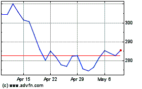
Cadence Design Systems (NASDAQ:CDNS)
Historical Stock Chart
From Oct 2024 to Nov 2024

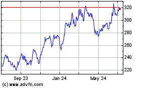
Cadence Design Systems (NASDAQ:CDNS)
Historical Stock Chart
From Nov 2023 to Nov 2024
