Media Alert: Cadence to Present and Showcase Technology at RTI's 3D Architectures for Semiconductor Integration and Packaging Co
December 06 2010 - 1:15PM
Marketwired
Cadence Design Systems, Inc. (NASDAQ: CDNS), a global leader in
electronic design innovation, today announced that the company will
be presenting a paper and showcasing its technology at RTI's 3D
Architectures for Semiconductor Integration and Packaging
conference. The conference will be Dec. 8 to 10 at the Hyatt
Regency San Francisco Airport Hotel in Burlingame.
WHAT: Cadence will demonstrate its 3D IC
and through-silicon vias (TSV) capabilities through videos and
demos at RTI's 3D Architectures for Semiconductor Integration and
Packaging conference. The tabletop demonstrations will be offered
throughout exhibition hours Dec. 9 and 10.
In addition, senior architect and technologist Vassilios
Gerousis will deliver a presentation with Damien Racquet of ST
Microelectronics on "3D IC Silicon Interposer Design Methodology."
That session will be held at 4:40 p.m. Dec. 9.
Journalists and bloggers interested in meeting with Cadence
representatives to discuss the latest advances in 3D IC technology
can call or email Dean Solov at 408-944-7226 or
dsolov@cadence.com.
3D IC can help speed Silicon Realization, a key tenet of the
EDA360 vision, and Cadence has been working aggressively to enhance
its product lines to enable more efficient 3D IC chip development.
The Encounter Digital Implementation System, for example, provides
an automated and integrated 3DIC/TSV implementation and analysis
design solution that supports timing, thermal, and signal integrity
analyses. This comprehensive set of technology includes 3DIC/TSV
floorplanning, automatic placement of the TSV, TSV net assignment,
optimization and re-distribution layer routing between the package
bumps and the TSV, and the TSV and the I/O pad cells.
The company has published a new white paper on 3D IC that will
available in hard copy at the conference and electronically at
www.cadence.com.
WHERE: RTI's 3D Architectures for
Semiconductor Integration and Packaging conference will be held at
the Hyatt Regency San Francisco Airport Hotel in Burlingame.
WHEN: The conference runs Dec. 8 to 10,
with Cadence technology on exhibition Dec. 9 and 10. The
presentation, "3D IC Silicon Interposer Design Methodology," will
be given at 4:40 p.m. Dec. 9.
About Cadence Cadence enables global
electronic design innovation and plays an essential role in the
creation of today's integrated circuits and electronics. Customers
use Cadence software and hardware, methodologies, and services to
design and verify advanced semiconductors, consumer electronics,
networking and telecommunications equipment, and computer systems.
The company is headquartered in San Jose, Calif., with sales
offices, design centers, and research facilities around the world
to serve the global electronics industry. More information about
the company, its products, and services is available at
www.cadence.com.
Cadence and the Cadence logo are registered trademarks of
Cadence Design Systems, Inc., in the United States and other
countries. All other marks and names are the property of their
respective owners
Add to Digg Bookmark with del.icio.us Add to Newsvine
For more information, please contact: Dean Solov Cadence
dsolov@cadence.com 408-944-7226
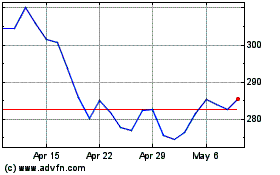
Cadence Design Systems (NASDAQ:CDNS)
Historical Stock Chart
From May 2024 to Jun 2024

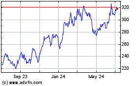
Cadence Design Systems (NASDAQ:CDNS)
Historical Stock Chart
From Jun 2023 to Jun 2024
