ACM Research Strengthens Atomic Layer Deposition Portfolio with Qualification of Thermal and Plasma-Enhanced ALD Furnace Tools
December 10 2024 - 4:05PM

ACM Research, Inc. (“ACM”) (NASDAQ: ACMR), a leading supplier of
wafer processing solutions for semiconductor and advanced packaging
applications, today announced the qualification of its Ultra Fn A
Plasma-Enhanced Atomic Layer Deposition (PEALD) Furnace tool. The
tool has achieved process qualification at a mainland China
semiconductor customer, and is now entering mass production. ACM
also announced that its Ultra Fn A Thermal Atomic Layer Deposition
(Thermal ALD) Furnace tool, introduced in 2022, has successfully
completed process qualification with another leading mainland China
customer, demonstrating performance parameters that it believes
match or exceed competitive tools.
“Modern integrated circuit (IC) manufacturing
increasingly relies on the deposition of ultra-thin films with
excellent step coverage and high quality,” said Dr. David Wang,
ACM’s President and Chief Executive Officer. “Addressing the
complexity of depositing materials such as silicon carbon nitride,
silicon nitride films, and low-k film requires true innovation, and
ACM’s R&D team has delivered with its ALD platforms and
processes. We believe ACM’s proprietary design is differentiated
from other suppliers and enables us to address challenges faced in
advanced 3D structure manufacturing.”
Both the Thermal ALD and PEALD configurations of
ACM’s Ultra Fn A Furnace ALD products can perform various film
deposition tasks such as hard mask, barrier, spacer, and sidewall
protection layers, supporting a range of requirements of target
process applications. Both configurations feature a six-unit system
capable of batch processing up to one-hundred 300mm wafers. The
tools also include four loadport systems with oxygen concentration
control in the loading area, an Integrated Gas Supply system (IGS),
and in-situ dry cleaning, all designed to meet SEMI standards.
Ultra Fn A PEALD Tool
ACM’s Ultra Fn A PEALD tool is designed for the
deposition of ultra-thin silicon nitride (SiN) films. It features a
double-layer tube with airflow balancing technology, which
significantly improves both wafer-in-wafer (WIW) and wafer-to-wafer
(WTW) uniformity. Using plasma-enhanced technology, the tool
effectively reduces the device's thermal budget. Furthermore, the
critical dimensions and pattern profiles of devices can be
precisely controlled by fine-tuning the precursors storage and
release amount to reaction tube.
Ultra Fn A Thermal ALD Tool
ACM’s Ultra Fn A Thermal ALD Tool has been
qualified for the deposition of silicon carbon nitride (SiCN)
films. It enables ultra-thin, void-free film deposition with
precise control over film thickness, achieving atomic-level
deposition accuracy. The tool also ensures precise carbon doping,
enhancing film hardness and improving corrosion resistance.
Additionally, it includes an in-situ dry cleaning step to maintain
particle stability, even when the film reaches low accumulated
thickness.
Forward-Looking Statements
Certain statements contained in this press
release are not historical facts and may be forward-looking
statements within the meaning of the Private Securities Litigation
Reform Act of 1995. Words such as “plans,” “expects,” “believes,”
“anticipates,” “designed,” and similar words are intended to
identify forward-looking statements. Forward-looking statements are
based on ACM management’s current expectations and beliefs and
involve a number of risks and uncertainties that are difficult to
predict and that could cause actual results to differ materially
from those stated or implied by the forward-looking statements. A
description of certain of these risks, uncertainties and other
matters can be found in filings ACM makes with the U.S. Securities
and Exchange Commission, all of which are available at www.sec.gov.
Because forward-looking statements involve risks and uncertainties,
actual results and events may differ materially from results and
events currently expected by ACM. Readers are cautioned not to
place undue reliance on these forward-looking statements, which
speak only as of the date hereof. ACM undertakes no obligation to
publicly update these forward-looking statements to reflect events
or circumstances that occur after the date hereof or to reflect any
change in its expectations with regard to these forward-looking
statements or the occurrence of unanticipated events.
About ACM Research, Inc.ACM
develops, manufactures and sells semiconductor process equipment
for single-wafer or batch wet cleaning, electroplating, stress-free
polishing, vertical furnace processes, Track and PECVD, which are
critical to advanced semiconductor device manufacturing and
packaging. ACM is committed to delivering customized,
high-performance, cost-effective process solutions that
semiconductor manufacturers can use in numerous manufacturing steps
to improve productivity and product yield. For more information,
visit www.acmr.com.
© ACM Research, Inc. ULTRA Fn and the ACM
Research logo are trademarks of ACM Research, Inc. For convenience,
these trademarks appear in this press release without ™ symbols,
but that practice does not mean ACM will not assert, to the fullest
extent under applicable law, its rights to such trademarks. All
other trademarks are the property of their respective owners.
| Media
Contact: |
Company
Contacts: |
| Alyssa Lundeen |
USA |
| Kiterocket |
Robert Metter |
| +1 218.398.0776 |
+1 503.367.9753 |
| alundeen@kiterocket.com |
|
| |
China |
| |
Xi Wang |
| |
ACM Research (Shanghai),
Inc. |
| |
+86 21 50808868 |
| |
|
| |
Korea |
| |
David Kim |
| |
ACM Research (Korea),
Inc. |
| |
+82 1041415171 |
| |
|
| |
Taiwan |
| |
David Chang |
| |
+886 921999884 |
| |
|
| |
Singapore |
| |
Adrian Ong |
| |
+65 8813-1107 |
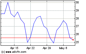
ACM Research (NASDAQ:ACMR)
Historical Stock Chart
From Dec 2024 to Jan 2025

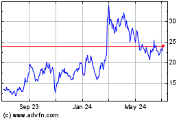
ACM Research (NASDAQ:ACMR)
Historical Stock Chart
From Jan 2024 to Jan 2025
