Advantest to Exhibit at IMAPS 2015, Orlando, FL, October 27-29
October 23 2015 - 9:00AM
Business Wire
Company to Showcase its Non-contact,
Non-destructive, TS9000 MTA, and NEW TDR Terahertz Analysis Systems
for Advanced ICs
Leading semiconductor test equipment supplier Advantest
Corporation (TSE:6857, NYSE:ATE) will promote its new TS9000
terahertz analysis systems for the semiconductor industry in Booth
619 at the International Microelectronics Assembly and Packaging
Society conference in Orlando, October 27-29, 2015. The TS9000 MTA
is an innovative metrology tool that automates mold overlay
thickness analysis for IC packaging using non-destructive pulsed
terahertz radiation, while the TS9000 TDR uses short-pulse
terahertz waves for analysis of electrical circuits in advanced
semiconductors. The TS9000 is part of the company’s family of
compact and multipurpose terahertz spectroscopic/imaging
systems.
The TS9000 MTA sets a new standard in the semiconductor industry
with its ability to perform mold thickness analysis of IC
packaging, previously difficult to measure using conventional
metrology. This “first-in-class” system enables rapid, repeatable
and highly accurate measurements, even when analyzing the optically
opaque mold polymer materials typically employed in IC packages.
The flexible system handles die in strip or singulated units and is
also fully compatible with industry-standard JEDEC trays.
Non-contact and non-destructive, it can be configured for partial
or 100% inspection of the product.
The TS9000 TDR, which utilizes short-pulse terahertz waves for
analysis of electrical circuits, provides analysis of circuit
errors with extremely high spatial precision of less than 5μm, and
a maximum measurement range of 300 mm, including internal circuits
such as through-silicon vias (TSVs) and interposers. Moreover, with
the optional TDR/TDT CAD Data Link, errors located can be mapped
and displayed on the CAD data of the target device, making it much
easier for users to identify the causes of errors. The new
technology overcomes the technical obstacles and prohibitive cost
of existing technologies, and will contribute significantly to the
development and wider adoption of these leading-edge devices.
IMAPS is the largest society dedicated to the advancement and
growth of microelectronics and electronics packaging technologies
through professional education. The conference will be held from
October 27-29, 2015 at the Rosen Center Hotel in Orlando, FL. More
information on IMAPS can be found at:
http://www.imaps.org/imaps2015/
About Advantest Corporation
A world-class technology company, Advantest is a leading
producer of automatic test equipment (ATE) for the semiconductor
industry and a premier manufacturer of measuring instruments used
in the design and production of electronic instruments and systems.
Its leading-edge systems and products are integrated into the most
advanced semiconductor production lines in the world. The company
also focuses on R&D for emerging markets that benefit from
advancements in nanotech and terahertz technologies, and has
introduced multi-vision metrology scanning electron microscopes
essential to photomask manufacturing, as well as a groundbreaking
3D imaging and analysis tools. Founded in Tokyo in 1954, Advantest
established its first subsidiary in 1982, in the USA, and now has
subsidiaries worldwide. More information is available at
www.advantest.com.
View source
version on businesswire.com: http://www.businesswire.com/news/home/20151023005100/en/
Advantest CorporationAmy Gold, +1
212.710.0515amy.gold@advantest.com
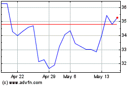
Advantest (PK) (USOTC:ATEYY)
Historical Stock Chart
From Nov 2024 to Dec 2024

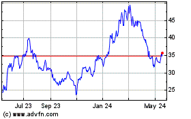
Advantest (PK) (USOTC:ATEYY)
Historical Stock Chart
From Dec 2023 to Dec 2024
