Cadence Unveils Holistic Approach to Silicon Realization
October 26 2010 - 12:00PM
Marketwired
Cadence Design Systems, Inc. (NASDAQ: CDNS), a global leader in
electronic design innovation, today introduced a new holistic
approach to Silicon Realization that moves chip development beyond
a patchwork of point tools to a streamlined end-to-end path of
integrated technology, tools, and methodology. This approach
represents a stark turn from the discreet and compartmentalized
ways semiconductor and systems companies have traditionally
achieved Silicon Realization, the term that refers to all the steps
required for bringing a design to silicon and a key component of
the EDA360 initiative.
The new Cadence® approach is focused on offering products and
technologies that deliver on the three requirements for a
deterministic path to silicon: unified design intent, design
abstraction and design convergence. A design flow that meets these
three requirements can deliver significant and measurable
productivity, predictability, and profitability boosts to chip and
systems makers facing today's greatest technology and business
challenges: mixed signal, low power, giga-gates/gigahertz,
verification, SiP and co-design, and global productivity and
metrics.
With new technology introduced today across the company's
Silicon Realization portfolio, Cadence® has made further
advancements to ensure its current and upcoming products meet these
three key requirements and can be incorporated into a holistic
flow. In the area of intent, new capabilities enable analog,
physical and electrical constraints to drive digital content into
mixed-signal flows and vice versa. For abstraction, design teams
now can create a die abstract for system-in-package and 3D IC
designs, bringing full interoperability between package and silicon
design. And for design convergence, Cadence introduced new
physical, electrical and functional links between logic design,
verification and implementation, providing greater convergence in
the design flow and allowing rapid ECOs. For more detailed
information, a Silicon Realization white paper is available for
download at
http://www.cadence.com/downloads/rl/wp/silicon_realization_wp.pdf.
"This approach reflects the best Cadence I've dealt with," said
Gary Smith, chief analyst for Gary Smith EDA. "Cadence continues to
define its strategy, has brought in good people and has tied their
performance to its strategic EDA360 goals. The intent is to tear
down the silos and have all of the company's divisions working with
each other. They are attempting to do what many other EDA companies
have tried and failed."
"In today's climate of complex designs and market pressures,
chip developers are in dire need of dramatic boosts in productivity
and profitability, and they simply can't get there by stitching
together tools from a dozen different vendors," said Chi-Ping Hsu,
Cadence senior vice president, research and development, Silicon
Realization Group. "Cadence's industry-leading, advanced low-power
solution first demonstrated our R&D teams' focus on building
tools that meet the requirements of unified design intent,
abstraction and convergence, and our future product releases will
continue to deliver on these core elements. Ultimately, we expect
to offer a number of seamless end-to-end design flows whose
built-in efficiencies will give customers a meaningful market
advantage."
About Cadence Cadence enables global
electronic design innovation and plays an essential role in the
creation of today's integrated circuits and electronics. Customers
use Cadence software and hardware, methodologies, and services to
design and verify advanced semiconductors, consumer electronics,
networking and telecommunications equipment, and computer systems.
The company is headquartered in San Jose, Calif., with sales
offices, design centers, and research facilities around the world
to serve the global electronics industry. More information about
the company, its products, and services is available at
www.cadence.com.
Cadence and the Cadence logo are registered trademarks of
Cadence Design Systems, Inc. in the United States and other
countries. All other trademarks are the property of their
respective owners.
Add to Digg Bookmark with del.icio.us Add to Newsvine
For more information, please contact: Dean Solov Cadence Design
Systems, Inc. 408-944-7226 dsolov@cadence.com
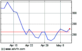
Cadence Design Systems (NASDAQ:CDNS)
Historical Stock Chart
From Oct 2024 to Nov 2024

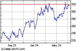
Cadence Design Systems (NASDAQ:CDNS)
Historical Stock Chart
From Nov 2023 to Nov 2024
