Sunplus Reduces Design Cycle on High-Speed Multi-Million-Gate SoC Using Cadence Encounter Digital Implementation System
September 27 2010 - 8:00PM
Marketwired
Cadence Design Systems, Inc. (NASDAQ: CDNS), a leader in global
electronic design innovation, today announced that Sunplus
Technology Co., Ltd. (TAIEX: 2401) (LSE: SUPD), a leading
multimedia IC design company, adopted the Cadence Encounter®
Digital Implementation (EDI) System for its multimedia
system-on-chip (SoC) designs.
"With EDI System, we achieved greater productivity and faster
time to market for our area-critical, high-performance 65-nanometer
designs," said Dr. Siuleong Yu, vice president and CTO of the Home
Entertainment Business Unit at Sunplus. "EDI System enabled us to
successfully tape out an advanced multimedia SoC design, involving
the incredibly complex integration of multi-million gates into a
single, low-power, area-efficient chip."
Today's consumer products are small, fast, feature-rich devices,
that are driving the demand for larger-scale, higher-performance,
complex low-power SoCs. To compete in this environment, Sunplus
must deliver state-of-the-art differentiated designs faster than
the competition. EDI System enables this by providing Sunplus with
a high performance, high-capacity scalable end-to-end digital
design solution to address the needs of high-density electronic
design.
"Cadence EDI System, a key element of our Silicon Realization
product line, delivers a significant advantage in productivity and
predictability for complex advanced node semiconductor designs,"
said Dr. Chi-Ping Hsu, senior vice president, Silicon Realization
Group at Cadence. "It is exciting to help leading customers like
Sunplus gain these advantages and to deliver new breakthrough
high-definition home-entertainment products with superior quality
and performance."
About Cadence Cadence enables global
electronic design innovation and plays an essential role in the
creation of today's integrated circuits and electronics. Customers
use Cadence software and hardware, methodologies, and services to
design and verify advanced semiconductors, consumer electronics,
networking and telecommunications equipment, and computer systems.
The company is headquartered in San Jose, Calif., with sales
offices, design centers, and research facilities around the world
to serve the global electronics industry. More information about
the company, its products, and services is available at
www.cadence.com.
Cadence, Encounter and the Cadence logo are registered
trademarks of Cadence Design Systems, Inc., in the USA and other
countries. All other marks and names are the property of their
respective owners
Add to Digg Bookmark with del.icio.us Add to Newsvine
For more information, please contact: Dean Solov Cadence Design
Systems, Inc. 408-944-7226 dsolov@cadence.com
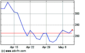
Cadence Design Systems (NASDAQ:CDNS)
Historical Stock Chart
From Oct 2024 to Nov 2024

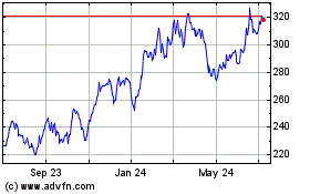
Cadence Design Systems (NASDAQ:CDNS)
Historical Stock Chart
From Nov 2023 to Nov 2024
