Applied Materials Solves Major Bottleneck to Continued 2D Scaling
July 20 2020 - 7:30AM

Applied Materials, Inc. today introduced a new technology that
removes a critical bottleneck to continued 2D scaling in
foundry-logic nodes.
Applied’s new Selective Tungsten process technology gives
chipmakers a new way to build transistor contacts, which are the
crucial, first level of wiring that connects the transistor to the
rest of the wiring in the chip. The selective deposition innovation
lowers contact resistance which impedes transistor performance and
increases power consumption. With this technology, node scaling of
transistors and their contacts can continue to 5nm, 3nm and below,
enabling simultaneous advances in chip power, performance and
area/cost (PPAC).
Scaling ChallengeWhile advances in lithography
have helped shrink the transistor contact vias, the traditional
approach to filling the vias with contact metal has become a
critical bottleneck to PPAC.
Traditionally, the transistor contacts have been formed in a
multi-layer process. The contact via is first lined with an
adhesion and barrier layer made of titanium nitride, then a
nucleation layer is deposited, and finally the remaining space is
filled with tungsten, which is the contact metal of choice due to
its low resistivity.
At the 7nm foundry node, the contact via is only about 20nm in
diameter. The liner-barrier and nucleation layers occupy
approximately 75 percent of the via’s volume, leaving only around
25 percent of the volume for tungsten. The thin tungsten wire has
very high contact resistance, and this creates a major bottleneck
to PPAC and further 2D scaling.
“With the arrival of EUV, we need to solve some critical
materials engineering challenges to enable 2D scaling to continue,”
said Dan Hutcheson, chairman and CEO of VLSIresearch.
“Liner-barriers have become our industry’s equivalent to arterial
plaque, robbing the chip of the flow of electrons it needs for peak
performance. Applied Materials’ selective tungsten is the
breakthrough we’ve been waiting for.”
Selective Tungsten DepositionApplied’s new
Endura® Volta™ Selective Tungsten CVD system enables chipmakers to
selectively deposit tungsten in the transistor contact vias,
eliminating the liner-barrier and nucleation layers. The entire via
is filled with low-resistance tungsten, and the bottleneck to
continued PPAC scaling is removed.
Applied’s Selective Tungsten technology is an Integrated
Materials Solution that combines multiple process technologies in a
pristine, high-vacuum environment that is many times cleaner than
the cleanroom itself. Atomic-level surface treatments are applied
to the wafer, and a unique deposition process is employed so that
tungsten atoms are selectively deposited in the contact vias,
creating a perfect bottom-up fill with no delamination, seams or
voids.
“For decades, the industry could count on 2D scaling to drive
simultaneous improvements in power, performance and area/cost,”
said Kevin Moraes, vice president, Semiconductor Products Group at
Applied Materials. “But today, the geometries are becoming so small
that we are hitting the physical limits of conventional materials
and materials engineering techniques. Our Integrated Materials
Solution for Selective Tungsten is a great example of how Applied
Materials is inventing new ways to shrink, without compromising
power and performance.”
The new Endura system has been selected by multiple leading
customers worldwide. It is the latest addition to Applied’s
portfolio of innovative selective process technologies which
include selective epitaxy, selective deposition and selective
removal. These selective processes allow chipmakers to create,
shape and modify materials in entirely new ways to enable continued
advances in PPAC.
About Applied Materials Applied Materials,
Inc. (Nasdaq: AMAT) is the leader in materials engineering
solutions used to produce virtually every new chip and advanced
display in the world. Our expertise in modifying materials at
atomic levels and on an industrial scale enables customers to
transform possibilities into reality. At Applied Materials,
our innovations make possible the technology shaping the future.
Learn more at www.appliedmaterials.com.
Contact:Ricky Gradwohl (editorial/media)
408.235.4676Michael Sullivan (financial community) 408.986.7977
A photo accompanying this announcement is available at
https://www.globenewswire.com/NewsRoom/AttachmentNg/e80b0739-8446-40c0-9bd2-cff27cd407f0
The photo is also available at Newscom, www.newscom.com, and via
AP PhotoExpress.
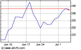
Applied Materials (NASDAQ:AMAT)
Historical Stock Chart
From Mar 2024 to Apr 2024

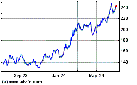
Applied Materials (NASDAQ:AMAT)
Historical Stock Chart
From Apr 2023 to Apr 2024
